
Modern smartphones are among the most advanced pieces of technology ever created. Inside every device are multiple semiconductor chips working together to deliver lightning-fast performance, crystal-clear photography, artificial intelligence, wireless communication, and exceptional battery life. While consumers often focus on the latest phone models, the real innovation happens deep inside the semiconductor fabrication process where these microscopic chips are manufactured.
For companies like Wafer Process Systems in San Jose, California, the production of these sophisticated semiconductor devices highlights the importance of precision cleaning and wet processing equipment throughout wafer fabrication. Even the smallest particle contamination can impact yield, reliability, and overall chip performance.
The Many Types of Chips Inside a Smartphone
A modern smartphone contains far more than a single processor. Instead, multiple specialized semiconductor devices work together to perform different functions.
The most recognizable is the System-on-Chip (SoC). This highly integrated chip combines the CPU, GPU, AI accelerator (often called an NPU), image signal processor, memory controllers, and other specialized processors onto a single piece of silicon. Today’s flagship SoCs are manufactured using advanced process nodes as small as 3nm or 5nm, allowing billions of transistors to fit onto an incredibly small surface area.
Smartphones also rely on several additional semiconductor components, including:
- DRAM memory for temporary high-speed data storage
- NAND Flash memory for long-term storage of applications, photos, and videos
- Power management integrated circuits (PMICs)
- Radio frequency (RF) chips for 5G, Wi-Fi, and Bluetooth connectivity
- CMOS image sensors for smartphone cameras
- Security processors for encryption and biometric authentication
- Display driver ICs that control OLED or LCD screens
Each of these chips performs a unique function, and together they create the seamless mobile experience users expect every day. Logic and memory devices make up a significant portion of semiconductor production for consumer electronics, with DRAM and NAND serving as the primary memory technologies used in smartphones.
Producing Smartphone Chips Is a Multi-Month Process
Manufacturing semiconductor chips is one of the most complex industrial processes in the world. Creating a finished wafer can require several months and hundreds or even thousands of individual process steps.
The process begins with an ultra-pure silicon wafer that serves as the foundation for every chip. Layers of materials are repeatedly deposited, patterned, etched, cleaned, and inspected to gradually build billions of microscopic transistors.
Photolithography transfers circuit patterns onto the wafer using advanced optical systems. Thin films are deposited to form insulating and conductive layers. Plasma etching removes unwanted material while ion implantation carefully modifies the electrical properties of the silicon.
One of the most overlooked—but absolutely essential—steps throughout fabrication is wafer cleaning.
Why Wafer Cleaning Is Critical
Every fabrication step introduces the possibility of contamination. Dust particles, metallic impurities, chemical residues, and microscopic defects can all reduce manufacturing yield or create failures that are impossible to detect until much later.
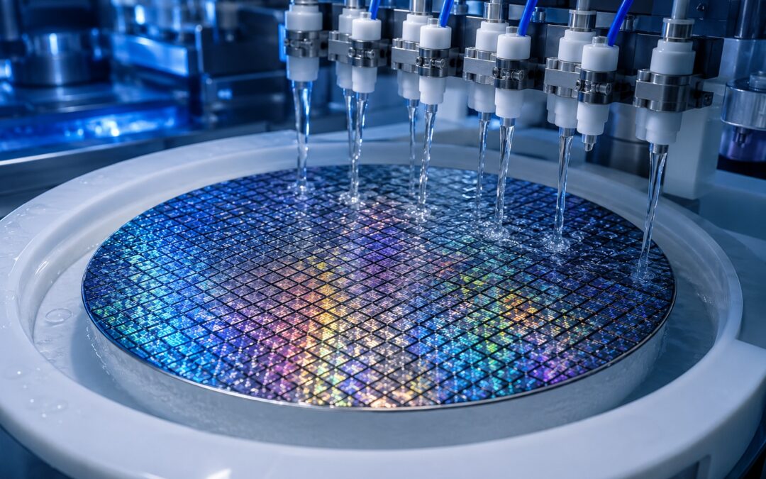
This is why wet processing and cleaning systems are integrated throughout semiconductor manufacturing. After many process steps, wafers are cleaned using carefully controlled chemical solutions that remove contaminants without damaging the delicate circuit structures.
Modern semiconductor fabs may clean a wafer dozens of times before manufacturing is complete. As feature sizes continue shrinking into the single-digit nanometer range, cleaning becomes even more important because contaminants that were once insignificant can now destroy microscopic transistor structures.
Companies such as Wafer Process Systems manufacture advanced wet bench equipment designed to automate these critical cleaning, rinsing, and chemical processing operations. Automated wet processing improves consistency, minimizes contamination risks, increases throughput, and helps semiconductor manufacturers maintain the exceptionally high yields required for today’s advanced devices.
Precision Manufacturing Makes Modern Smartphones Possible
After fabrication is complete, wafers undergo extensive inspection and electrical testing before being diced into individual chips. These dies are then packaged, tested again, and integrated into smartphone circuit boards where they work together to power every feature users depend on—from AI-powered photography to high-speed 5G communication and immersive mobile gaming.
As semiconductor technology continues to evolve, manufacturers are pushing toward even smaller process nodes, more advanced packaging technologies, and increasingly complex chip architectures. Every advancement places greater demands on fabrication equipment, contamination control, and process precision.
For companies like Wafer Process Systems, precision wet processing equipment remains a vital part of the semiconductor manufacturing ecosystem. By helping fabs maintain ultra-clean wafer surfaces throughout production, advanced wet bench systems contribute directly to the quality, reliability, and performance of the semiconductor chips that power millions of smartphones around the world every day.